o ANDES Advanced Superscalar Architecture
- Supports Four Instructions per Cycle
- Two Integer and Two Floating Point Execute Instructions Plus One Load/Store per Cycle
o High Performance Design
- 200 MHz Internal Clock Rate
- 3.3 Volt Technology
- Out-of-Order Instruction Execution
- 128-bit Dedicated Secondary Cache Data Bus
- On-Chip Integer, FP, and Address Queues
- Five Separate Execution Units
- MIPS IV Instruction Set Architecture
o High Integration Chip-Set
- 32 KByte 2-way Set Associative, 2-way Interleaved Data Cache with LRU Replacement Algorithm
- 32 KByte 2-way Set Associative Instruction Cache
- 64 Entry Translation Lookaside Buffer
- Dedicated Second Level Cache Support
o Second Level Cache Support
- Dedicated 128-bit Data Bus
- Generation of all necessary SSRAM signals
- 3.2 GBytes/second peak data transfer rate
- Up to 200 MHz SSRAM interface
- Programmable Clock Rate to SSRAM
o Compatible with Industry Standards
- ANSI/IEEE Standard 754-1985 for Binary Floating Point Arithmetic
- MIPS III Instruction Set Compatible
- Conforms to MESI Cache Consistency Protocol
- IEEE Standard 1149.1/D6 Boundary Scan Architecture
o Avalanche Bus System Interface
- Direct Connect to SSRAM
- Split Transaction Support
- Programmable Interface
The R10000 Microprocessor from MIPS Technologies is a 4-way super-scalar architecture which fetches and decodes four instructions per cycle. Each decoded instruction is appended to one of three instruction queues. Each queue can perform dynamic scheduling of instructions. The queues determine the execution order based on the availability of the required execution units. Instructions are initially fetched and decoded in order, but can be executed and completed out-of-order, allowing the processor to have up to 32 instructions in various stages of execution. The impressive integer and floating point performance of the R10000 Microprocessor makes it ideal for applications such as engineering workstations, scientific computing, 3-D graphics workstations, database servers, and multi-user systems. The high throughput is achieved through the use of wide, dedicated data paths, and large on- and off- chip caches.
The R10000 Microprocessor implements the MIPS IV instruction set architecture. MIPS IV is a superset of the MIPS III instruction set architecture and is backward compatible. At a frequency of 200 MHz, the R10000 Microprocessor delivers peak performance of 800 MIPS with a peak data transfer rate of 3.2 GBytes/second to secondary cache. The R10000 Microprocessor is available in a 599 CLGA package and is fabricated using a CMOS sub .35-micron silicon technology.
1 MODERN COMPUTING CHALLENGES
The current generation of today's microprocessor architectures outperform their earlier counterparts by orders of magnitude. Such radical increases in performance, speed, and transistor count from generation to generation, often separated by only a few years, can seem overwhelming to the casual observer. In many cases speeds and transistor counts have increased by an order of magnitude just since the late 1980's.
Although current microprocessor designs vary greatly, there are many commonalities between them. Each one performs address generation, each contains arithmetic logic units, register files, and a system interface. Most have on-chip caches, a translation lookaside buffer (TLB), and almost all current architectures have on-chip floating point units.
Many different design techniques have been used to perform these basic functions, but the sheer nature and existence of these functions and the need to perform them lend themselves to inherent problems that must be overcome. This section discusses some of the common computing challenges faced by all microprocessor designers. Section two discusses some of the techniques used to overcome these challenges. Section 3 discusses how the MIPS R10000 microprocessor implements the techniques discussed in section 2.
1.1 MEMORY AND SECONDARY CACHE LATENCIES
Early microprocessors had to fetch instructions directly from memory. Historically, memory access times have lagged far behind the data-rate requirements of the processor. After issuing a request for data the processor was forced to wait long periods of time for the data to return. This severely hampered the processor's ability to operate efficiently at the speeds for which it was designed.
The implementation of off-chip secondary cache memory systems have helped to alleviate this problem. A cache memory system is comprised of a small amount of memory, normally 32K-256 KBytes, which contains a block of memory addresses comprising a small section of main memory. Cache memory has much faster access times and can deliver data to the processor at a much higher rate than main memory.
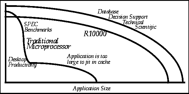
On-chip cache memory systems can greatly improve processor performance because they allow accesses to be completed often times in one cycle. The performance improvements of on-chip cache systems have caused many architectures to dedicate increasing amounts of space and logic to cache design. In many current designs the cache system requires as much as 50% of the total die. Performance is highest when the application is able to run within the cache. However, when the application is too large to fit into the cache performance decreases significantly. Figure 1 shows the relationship between application performance and size.
Figure 1 Application Performance versus Size
The on-chip cache contains a range of addresses which comprise a subset of those addresses in the secondary cache. In turn, the secondary cache contains a range of addresses which comprise a subset of those addresses in main memory. Figure 2 shows the relationship between caches in a typical computer system.
As beneficial as on-chip cache systems are to processor performance, current semiconductor technology and available transistor counts limit cache size. Currently 64 KBytes (32K Data, 32K Instruction) is a large on-chip cache requiring several million transistors to implement.
The limiting size factors regarding on-chip caches place increasing importance on secondary cache systems, where cache size is only limited by the market into which the product is being sold. However, cache memory is not without its limitations.
The access times of most currently available RAM devices are long relative to processor cycle times and force the memory system designer to find ways to hide them. Interleaving the cache system is one way to accomplish this. Interleaved cache memory systems allow processor memory requests to be overlapped. Both cache and main memory can be interleaved. Two and four way interleaving is common in memory systems. Increasing the amount of interleaving allows the ability to hide more of the access and recovery times of each bank, but increased complexity is required to support them. Refer to section 2.3 for a further discussion of memory interleaving.
1.2 DATA DEPENDENCIES
In a computer program, instructions are fetched from the instruction cache, decoded, and executed. The corresponding data is often fetched from a register, manipulated within an ALU, and the result placed either in the same register or perhaps in another register.
If the next instruction in the sequence requires the result of the previous instruction before it can execute, a data dependency occurs. For instructions which require many cycles to complete, performance can be adversely impacted as the execution of the second instruction must wait until the first instruction has completed and the result written to the register. Some dependencies can be eliminated simply by re-arranging the program so that the result of a given instruction is not used by the next few instructions.
Out-of-order execution using register renaming helps to alleviate the data dependency problem. Register renaming is explained in section 2.1.
1.3 BRANCHES
All computer programs contain branches. Some branches are unconditional, meaning that the program flow is interrupted as soon as the branch instruction is executed. Other branches are conditional, meaning that the branch is taken only if certain conditions are met. Program flow interruption is inherent to all computer software and the microprocessor hardware has little choice but to deal with branches in the most efficient way possible.
When a branch is taken, the new address at which the program is to resume may or may not reside in the secondary cache. The latency is increased depending on where the new instruction block is located. Since the access times of the main memory and secondary cache are far greater than the on-chip cache, as shown in figure 2, branching can often degrade processor performance.
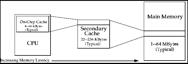
Figure 2 Memory Relationships in a Typical Computer System
The branching problem is further compounded in super-scalar machines where multiple instructions are fetched every cycle and progress through stages of a pipeline toward execution. At any given time, depending on the size of the pipeline, numerous instructions can be in various stages of execution. When a conditional branch instruction is executed it is not known until many cycles later when the instruction is actually executed whether or not the branch should have been taken.
Implementation of branching is an important architectural problem. To improve performance many current architectures incorporate branch prediction circuitry, which can be implemented in a number of ways. Section 2.2 discusses some commonly used branch prediction techniques.
2 TOLERATING MEMORY LATENCY
As explained in section 1, memory latency reduction is a critical issue in increasing processor performance. This section discusses some of the common architectural techniques used to reduce memory latency.
2.1 High Bandwidth Secondary Cache Interface
The ideal secondary cache interface would be one where the cache receives a data request from the processor and would always be able to return data in the following clock. This is referred to as a true zero wait state cache. In order to design a secondary cache which can approach zero wait state performance, the design of the processor's system interface must be designed such that data can be transferred at the maximum rate allowed.
The address and data busses of most processor's interface to the entire computer system. Any number of different devices can be accessed by the processor at any given time.
Whenever an on-chip cache miss occurs, an address is driven out onto the bus and the secondary cache is accessed, transferring the requested data to the on-chip cache.
If an on-chip cache miss occurs in a shared bus system, and the processor is using the external bus to read or write some other device, the access to secondary cache must wait until the external data and address busses are free. This can take many cycles depending on the peripheral being accessed.
In a dedicated bus system the data, address, and control busses for the secondary cache are separate from those which interface to the rest of the system. These busses allow secondary cache accesses to occur immediately following an on-chip cache miss, regardless of what else is happening in the system.
Figure 3 shows a block diagram of both a shared and dedicated secondary cache interface. Refer to section 3.9 for more information on the dedicated secondary cache interface of the R10000 microprocessor.
2.2 Block Accesses
When an on-chip cache miss occurs there is normally a programmable number of bytes which are transferred each time the secondary cache is accessed. This number is referred to as the cache line size. Thirty-two bytes is a common line size for many current architectures.
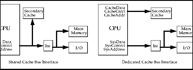
Figure 3 Dedicated Secondary Cache Bus Interface
The number of accesses required to perform a line fill depends on the size of the external data bus of the processor. For example, a processor with a 64 bit data bus interfacing to a 64-bit wide memory and performing a 32 byte (256 bits) cache line fill would require four secondary cache accesses to fetch all of the data. To accomplish this the processor must generate 4 separate addresses and drive each one out onto the external address bus, along with the appropriate control signals.
Block access mode allows the processor to generate only the beginning address of the sequence. The remaining three addresses are generated either by cache control logic, or within the cache RAM itself. The R10000 microprocessor system interface supports block accesses.
2.3 Interleaved Memory
Interleaving is a design technique used to increase memory bandwidth. The concept of interleaving can be applied both to secondary cache and main memory.
The simplest memory system has one bank of memory. If the memory is accessed some amount of time must elapse before the memory can be accessed again. This time depends both on the system design as well as the speed of the memory devices being used. Having multiple banks allows for bank accesses to be overlapped. The ability to overlap bank accesses helps to hide these inherent memory latencies and becomes increasingly important as the amount of data requested increases.
A typical interleaved memory system consists of even and odd banks. For example, the processor places a request for data at an even address. The memory controller then initiates a cycle to the even bank. Once the address has been latched by the memory control logic, the processor is free to generate a new address, often times in the next clock. If the new address is to the odd bank of memory, the memory access can begin immediately as the odd bank is currently idle. By the time the access time to the even bank has elapsed and the corresponding data has been returned, the odd bank is also ready to return data. Zero wait state performance can potentially be achieved as long as sequential accesses to the same bank are kept to a minimum.
Two-way and four-way interleaved memory systems are the most common. The number of banks and the data bandwidth of each is often determined by the processor. For example, if the cache line size of the processor is 32 bytes, this means that each time a memory access is initiated 32 bytes must be returned to the processor. Since 32 bytes = 256 bits, a common approach is to have four banks of 64 bits each. This scheme would require a processor with a 64-bit data bus in order to alleviate any external multiplexing of data. Each bank is accessed in an order determined by the processor. Section 3.1 discusses the interleaving characteristics of the R10000 microprocessor.
2.4 Non-Blocking Cache
In a typical implementation, the processor executes out of the cache until a cache miss is taken. A number of cycles elapse before data is returned to the processor and placed in the on-chip cache, allowing execution to resume. This type of implementation is referred to as a blocking cache because the cache cannot be accessed again until the cache miss is resolved.
Non-blocking caches allow subsequent cache accesses to continue even though a cache miss has occurred. Locating cache misses as early as possible and performing the required steps to solve them is crucial in increasing overall cache system performance. Figure 4 shows an example of how a blocking and non-blocking cache would react to multiple cache misses.
The major advantage of a non-blocking cache is the ability to stack memory references by queuing up multiple cache misses and servicing them simultaneously. The sooner the hardware can begin servicing the cache miss, the sooner data can be returned.
2.5 Prefetch
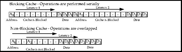
Figure 4 Multiple Misses in a Blocking and Non-Blocking Cache
Prefetching of instructions is a technique whereby the processor can request a cache block prior to the time it is actually needed. The prefetch instruction must be integrated as part of the instruction set and the appropriate hardware must exist to execute the prefetch instruction.
For example, assume the compiler is progressing sequentially through a segment of code. The compiler can make the assumption that this sequence will continue beyond the range of addresses available in the on-chip cache and issue a prefetch instruction which fetches the next block of instructions in the sequence and places them in the secondary cache. Therefore, when the processor requires the next sequence, the block of instructions exist in the secondary cache or a special instruction buffer as opposed to main memory and can be fetched by the processor at a much faster rate. If for some reason the block of instructions is not needed, the area in the secondary cache or the buffer is simply overwritten with other instructions.
Prefetching allows the compiler to anticipate the need for a given block and place it as close to the CPU as possible.
DATA DEPENDENCY
Two common techniques are used to reduce the negative performance impact of data dependencies. Each of these is discussed below.
2.6 Register Renaming
Register renaming distinguishes between logical registers, which are referenced within instruction fields, and physical registers, which are located in the hardware register file. Logical registers are dynamically mapped into physical register numbers using mapping tables which are updated after each instruction is decoded. Each new result is written into a new physical register. However, the previous contents of each logical register is saved and can be restored in case its instruction must be aborted following an exception or an incorrect branch prediction.
As the processor executes instructions a myriad of temporary register results are generated. These temporary values are stored in register files along with permanent values. The temporary values become new permanent values when the corresponding instructions graduates. An instruction graduates when all previous instructions have been successfully completed in program order.
The programmer is aware of only logical registers. The implementation of physical registers is hidden. Logical register numbers are dynamically mapped into physical register numbers. The mapping is implemented using mapping tables which are updated after each instruction is decoded. Each new result is written into a physical register. However, until the corresponding instruction graduates, the value is considered temporary.
Register renaming simplifies data dependency checks. In a machine which can execute instructions out-of-order, logical register numbers can become ambiguous as the same register may be assigned a succession of different values. But because physical register numbers uniquely identify each result, dependency checking becomes unambiguous. Section 3.6. discusses how the R10000 microprocessor implements register renaming.
2.7 Out-of Order Execution
In a typical pipelined processor which executes instructions in-order, each instruction depends on the previous instruction which produced its operands. Execution cannot begin until those operands become valid. If the operands required to execute a given instruction are not valid, the pipeline stalls until those operands become valid. Because instructions execute in order, stalls usually delay all subsequent instructions.
In an in-order superscalar machine where multiple instructions are fetched each cycle, several consecutive instructions can begin execution simultaneously if all of their corresponding operands are valid. However, the processor stalls at any instruction whose operands are not valid.
In an out-of-order superscalar machine each instruction is eligible to begin execution as soon as its operands become available regardless of the original instruction sequence. The hardware effectively re-arranges instructions in order to keep the various execution units busy. This process is called dynamic issuing. Section 3.6.1 discusses the out-of-order implementation used in the R10000 microprocessor.
BRANCH PREDICTION
As stated in section 1.3, branches interrupt the pipeline flow. Therefore, branch prediction schemes are needed to minimize the number of interruptions. Branches occur frequently, averaging about one out of every six instructions. In super-scalar architectures where more than one instruction at a time is fetched, branch prediction becomes increasingly important. For example, in a four-way super-scalar architecture, where four instructions per cycle are fetched, a branch instruction can be encountered every other clock.
Most branch prediction schemes use algorithms which keep track of how a conditional branch instruction behaved the last time it was executed. For example, if the branch history circuit shows that the branch was taken the last time the instruction was executed, the assumption could be made that it will be taken again. A hardware implementation of this assumption would mean that the program would vector to the new target address and that all subsequent instruction fetches would occur at the new address. The pipeline now contains a conditional branch instruction fetched from some address, and numerous instructions fetched afterward from some other address. Therefore, all instructions fetched between the time the branch instruction is fetched and the time it is executed are said to be speculative. That is, it is not known at the time they are fetched whether or not they will be completed. If the branch was predicted incorrectly, the instructions in the pipeline must be aborted.
Many architectures implement a branch stack which saves alternate addresses. If the branch is predicted to be not-taken, the address of the actual branch instruction is saved. If the branch is predicted to be taken, the address immediately following the branch instruction is saved. Section 3.4 discusses the branch mechanism of the R10000 microprocessor.
3 R10000 PRODUCT OVERVIEW
The R10000 Microprocessor implements many of the techniques mentioned above. This section discusses some of these features. Figure 5 shows a block diagram of the R10000 microprocessor.
3.1 PRIMARY DATA CACHE
The primary data cache of the R10000 Microprocessor is 32K bytes in size and is arranged as two identical 16K-byte banks. The cache is two-way interleaved. Each of the two banks is two-way set associative. Cache line size is 32 bytes.
The data cache is virtually indexed and physically tagged. The virtual indexing allows the cache to be indexed in the same clock in which the virtual address is generated. However, the cache is physically tagged in order to maintain coherency with the secondary cache.
3.2 SECONDARY DATA CACHE
The secondary cache interface of the R10000 Microprocessor provides a 128-bit data bus which can operate at a maximum of 200 MHz, yielding a peak data transfer rate of 3.2 GBytes/second. All of the standard Synchronous Static RAM interface signals are generated by the processor. No external interface circuitry is required. The minimum cache size is 512K Bytes. Maximum cache size is 16 MBytes. Secondary cache line size is programmable at either 64 or 128 bytes.
3.3 INSTRUCTION CACHE
The instruction cache is 32K Bytes and is two-way set associative. Instructions are partially decoded before being placed in the instruction cache. Four extra bits are appended to each instruction to identify which execution unit the instruction will be dispatched to. The instruction cache line size is 64 bytes.
3.4 BRANCH PREDICTION
The branch unit of the R10000 Microprocessor can decode and execute one branch instruction per cycle. Since each branch is followed by a delay slot, a maximum of two branch instructions can be fetched simultaneously, but only the earlier one will be decoded in a given cycle.
A branch bit is appended to each instruction during instruction decode. These bits are used to locate branch instructions in the instruction fetch pipeline.
The path a branch will take is predicted using a branch history RAM. This two-bit RAM keeps track of how often each particular branch was taken in the past. The two-bit code is updated whenever a final branch decision is made.
Any instruction fetched after a branch instruction is speculative, meaning that it is not known at the time these instructions are fetched whether or not they will be completed. The R10000 Microprocessor allows up to 4 outstanding branch predictions which can be resolved in any order.
Special on-chip branch stack circuitry contains an entry for each branch instruction being speculatively executed. Each entry contains the information needed to restore the processor's state if the speculative branch is predicted incorrectly. The branch stack allows the processor to restore the pipeline quickly and efficiently when a branch mis-prediction occurs.
3.5 QUEUEING STRUCTURES
The R10000 Microprocessor contains three instruction queues. These queues dynamically issue instructions to the various execution units. Each queue uses instruction tags to track instructions in each execution pipeline stage. Each queue performs dynamic scheduling and can determine when the operands that each instruction needs are available. In addition, the queues determine the execution order based on the availability of the corresponding execution units. When the resources become available the queue releases the instruction to the appropriate execution unit.
3.5.1 Integer Queue
The integer queue contains 16 entries and issues instructions to the two integer arithmetic logic units. Integer instructions are written into empty queue entries and up to four entries may be written each cycle. Integer Instructions remain in the queue until being issued to an ALU.
3.5.2 Floating Point Queue
The floating point queue contains 16 entries and issues instructions to the floating-point adder and floating-point multiplier execution units. Floating Point instructions are written into empty queue entries and up to four entries may be written each cycle. Instructions remain in the queue until being issued to an execution unit. The floating-point queue also contains multiple-pass sequencing logic for instructions such as the multiply-add. This instruction is dispatched first to the multiply unit, then passed directly to the adder unit.
3.5.3 Address Queue
The address queue issues instructions to the Load-Store unit and contains 16 entries. The queue is organized as a circular FIFO (first-in first-out) buffer. Instructions can be issued in any order, but must be written to or removed from the queue in sequential order. Up to four instructions can be written every cycle. The FIFO maintains the programs original instruction sequence so that memory address dependencies may be computed easily.
An issued instruction may fail to complete because of a memory dependency, a cache miss, or a resource conflict. In these cases the address queue must re-issue the instruction until it is completed.
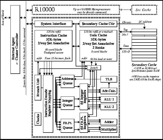
Figure 5 R10000 Microprocessor Block Diagram
3.6 REGISTER RENAMING
Dependencies between instructions can degrade the overall performance of the processor. Register renaming is a technique used to determine these dependencies between instructions and provide for precise exception handling. When a register is renamed the logical registers which are referenced in an instruction are mapped to physical registers using a mapping table. A logical register is mapped to a new physical register whenever it is the destination of an instruction. Hence when an instruction puts a new value in a logical register, that logical register is renamed to use the new physical register. However, the previous value remains in the old physical register. Saving the old register value allows for precise exception handling.
While each instruction is renamed, its logical register numbers are compared to determine the dependencies between the four instructions being decoded during the same cycle.
3.6.1 Mapping Tables
The instruction mapping scheme implemented in the R10000 microprocessor consists of a mapping table, an active list, and a free list. Separate mapping tables and free lists are provided for integer and floating-point instructions. To maintain sequential ordering of instructions, only one active list exists which contains both integer and floating-point instructions.
The R10000 Microprocessor contains 64 physical registers. At any given time each physical register value is contained within one of these lists. Figure 6 shows a block diagram of the integer instruction mapping scheme.
Instructions are fetched from the instruction cache and placed in the mapping table shown in figure 6. At any given time each of the 64 physical registers is located in one of these three blocks.
The active list maintains a listing of all 32 instructions in the pipeline at any given time. This list is always in order. The instructions in the queues can be executed out-of-order, but before the value can be stored as final, the result must be stored in order as determined by the active list. Once the value is stored it becomes obsolete and is no longer active. The logical destination can then be returned to the free list.
Each instruction can be uniquely identified by its location within the active list. A 5-bit value called the instruction's tag accompanies each instruction and allows it to be easily located within the 32-instruction active list so that it can be marked as done when the instruction graduates
When a value is taken from the free list it is passed to the mapping table and the mapping table updated. The particular register value now contains the current value of an operand. The old value from the mapping table is then placed on the active list. The value remains on the active list until the instruction graduates, meaning that it has been completed in program order. An instruction can graduate only after it and all previous instructions have been successfully completed. Once an instruction has graduated, all previous values are lost.
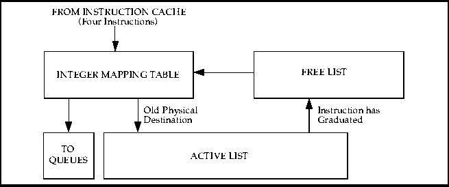
Figure 6 Integer Instruction Mapping Scheme Block Diagram
The R10000 Microprocessor contains 64 physical registers and 32 logical registers. The active list can contain a maximum of 32 values. The free list can also contain a maximum of 32 values. If the active list is full there could be 32 committed values and 32 temporary values, hence the need for 64 physical registers.
3.7 EXECUTION UNITS
The R10000 Microprocessor contains five execution units which operate independently of one another. There are two integer arithmetic logic units (ALU), two primary floating-point units, and two secondary FP units which handle long-latency instructions such as divide and square root.
3.7.1 Integer ALU's
There are two integer ALU's in the R10000 Microprocessor defined as ALU1 and ALU2. Integer ALU operations, with the exception of the multiply and divide operations, execute with a 1-cycle latency and a 1-cycle repeat rate.
Both ALU's perform standard add, subtract, and logical operations. These operations complete in one cycle. ALU1 handles all branch and shift instructions, while ALU2 handles all multiply and divide operations using iterative algorithms. Integer multiply and divide instructions place their results in the EntryHi and EntryLo registers.
During multiply operations other single-cycle instructions can be executed within ALU2 while the multiplier is busy. However, once the multiplier has finished, ALU2 is busy for two cycles while the result is stored in two registers. For divide operations which have extra long latencies ALU2 is busy for the duration of the operation.
Integer multiply operations generate a double-precision product. For single-precision operations the result is sign-extended to 64 bits before being placed in the EntryHi and EntryLo registers. Double-precision latencies are approximately twice that of single precision. Refer to table 1.
3.7.2 Floating-Point Units
The R10000 Microprocessor contains two primary floating point units. The adder unit handles add operations and the multiply unit handles multiply operations. In addition, two secondary floating point units exist which handle long-latency operations such as divide and square root.
Addition, subtraction, and conversion instructions have a 2-cycle latency and a 1-cycle repeat rate and are handled within the adder unit. Instructions which convert integer values to single-precision floating point values have a 4-cycle latency as they must pass through the adder twice. The adder is busy during the second cycle after the instruction is issued.
All floating-point multiply operations execute with a 2-cycle latency and a 1-cycle repeat rate and are handled within the multiplier unit. The multiplier performs multiply operations. The floating-point divide and square root units perform calculations using iterative algorithms. These units are not pipelined and cannot begin another operation until the current operation is completed. Thus, the repeat rate approximately equals the latency. The ports of the multiplier are shared with the divide and square root units. A cycle is lost at the beginning of the operation (to fetch the operand) and at the end (to store the result).
The floating point multiply-add operation, which occurs frequently, is computed using separate multiply and add operations. The multiply-add instruction (MADD) has a 4-cycle latency and a 1-cycle repeat rate. The combined instruction improves performance by eliminating the fetching and decoding of an extra instruction.
The divide and square root units use separate circuitry and can be operated simultaneously. However, the floating-point queue cannot issue both instructions during the same cycle.
Table 1 shows the latency and repeat rates for the integer and floating point units.
3.8 LOAD/STORE UNITS AND THE TLB
The Load/Store unit consists of the address queue, address calculation unit, translation lookaside buffer (TLB), address stack, store buffer, and primary data cache. The Load/Store unit performs load, store, prefetch, and cache instructions.
All load or store instructions begin with a 3-cycle sequence which issues the instruction, calculates its virtual address, and translates the virtual address to physical. The address is translated only once during the operation. The data cache is accessed and the required data transfer is completed provided there was a primary data cache hit.
If there is a cache miss, or if the necessary shared register ports are busy, the data cache and data cache tag access must be repeated after the data is obtained from either the secondary cache or main memory.
The TLB contains 64 entries and translates virtual addresses to physical addresses. The virtual address can originate from either the address calculation unit or the program counter (PC).
3.9 SECONDARY CACHE INTERFACE
Secondary cache support for the R10000 Microprocessor is provided by an internal secondary cache controller with a dedicated secondary cache port. A dedicated 128-bit bus transfers data at the 200 MHz internal operating frequency of the R10000 CPU, yielding a maximum secondary cache data transfer rate of 3.2 GBytes/second. The R10000 Microprocessor also provides a 64-bit system interface data bus.
The secondary cache is implemented as two-way set associative. Maximum cache size is 16 MBytes. Minimum cache size is 512 KBytes. Transfer width is 128 bits, or (4) 32-bit words. Consecutive cycles are used to transfer larger blocks of data as shown below.
-- Four word accesses (128 bits) are used for the CACHE instruction.
-- Eight word accesses (256 bits) are used for primary data cache refills & write backs.
-- Sixteen word accesses (512 bits) are used for primary instruction cache refills; and SCache refills & write backs (if SCache line size is selected to be 16Words).
-- Thirty-two word accesses (1024 bits) are used for secondary cache refills & write backs (if SCache Line Size is selected to be 32 words).
3.10 SYSTEM INTERFACE
The system interface of the R10000 Microprocessor provides a gateway between the R10000 and its associated secondary cache, and the rest of the computer system. The system interface operates at the frequency of SysClk being supplied to the processor. The programmability of the system interface allows for clock speeds of 200, 133, 100, 80, 67, 57, and 50 MHz. All system interface outputs, as well as all inputs, are clocked on the rising edge of SysClk, allowing the system interface to run at the highest possible clock frequency.
In most microprocessor systems only one system transaction can occur at any given time. The R10000 Microprocessor supports a split-level bus transaction protocol. Split-transaction allows additional processor and external requests to be issued while waiting for a previous response. A maximum of four outstanding transactions at any given time are supported (see below).
3.10.1 Multi-Processor Support

Table 1: Instruction Latencies and Repeat Rates
------------------------------------------------------------------------------------ Instruction Latency Repeat Rate------------------------------------------------------------------------------------ Integer Add, Subtract, Logical Op's, branches 1 1 Integer Load/Store (primary cache hit) 2 1 Integer Multiply (single precision) 5 (Lo) - 6 (Hi) 6 Integer Multiply (double precision) 9 (Lo) -10 (Hi) 10 Integer Divide (single precision) 34 (Lo) - 35 (Hi) 35 Integer Divide (double precision) 66 (Lo) - 67 (Hi) 67 Integer to FP conversion (single precision) 4 1 Floating Point Add, Subtract, Conversion, Logical 2 1 operations Floating Point Load/Store 3 1 Floating Point Multiply (double precision) 2 1 Floating Point Multiply-Add 2/4 1 Floating Point Divide (single precision) 12 14 Floating Point Divide (double precision) 19 21 Floating Point Square Root (single precision) 18 20 Floating Point Square Root (double precision) 33 35 Floating Point Reciprocal Square Root (single prec.) 30 20 Floating Point Reciprocal Square Root (double prec.) 52 35 ------------------------------------------------------------------------------------
Table 1: Revised on September 1, 1995
Two configurations of multi-processor systems can be implemented using the R10000 microprocessor. One way is to have a dedicated external agent interface to each processor. The external agent is typically an ASIC which provides a gateway to the memory and I/O subsystems. In this type of configuration the processors do not interface directly together but rather through each external agent. Although this implementation is commonly used, cost as well as overall system complexity are increased due to the fact that at least one external agent must accompany each processor.
The R10000 microprocessor provides pin support for a cluster bus configuration. In a cluster configuration up to four R10000 CPU's may be connected together via a cluster bus. Only one external agent is then required to interface to other system resources. Each processor interfaces to the same external agent. The cluster-bus implementation reduces not only the complexity but the number of ASIC's, and hence the cost of the system by requiring only one external agent per four processors.
In addition to the 64-bit multiplexed address/data bus, a 2-bit state bus is provided which is used for issuing processor coherency state responses. Also, a 5-bit system response bus is used by the external agent for issuing external completion responses. Figure 7 shows a block diagram of a cluster bus configuration.
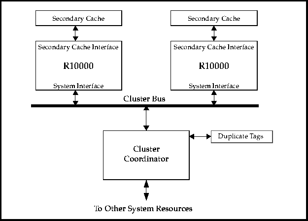
Figure 7 Multi-processor System using the Cluster Bus